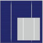
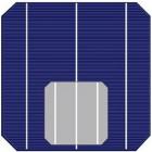
6"单晶硅片
产品特点:
单晶硅片
P-型
硼掺杂
准方
156 x 156 mm
厚度: 200 ± 20 μm
Mono-crystalline Wafer
A wafer is generally a thin slice of
semiconductor material (e.g. silicon crystal) used in the fabrication of
integrated circuits and other micro devices. Undergoing many micro fabrication
process steps such as doping or ion implantation, the wafer serves as the
substrate for microelectronic devices built in and over the wafer. Several
types of solar cells are made from such wafers.
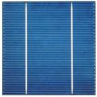
A solar wafer is a circular solar cell
made using the entire wafer instead of cutting it into smaller, rectangular
solar cells. Made from high-purity silicon, the ingot is prepared to produce
the wafer. One process used to produce mono-crystalline wafers is known as
Czochralski Growth, which was invented by the Polish chemist, Jan Czochralski.
In this process, a cylindrical ingot of high-purity, crystalline silicon is
formed by pulling a seed crystal from a "melt." The surface of the
wafer aligns in one of several relative directions known as crystal
orientations. Orientations of solar wafers are defined by the miller index with
type [100]s being the most common for silicon. These are prepared into stacks
which are in turn cut into very thin discs (wafers) with the help of modern
wire-cutting technology.
After cleaning and intensive final
checks, the mono-crystalline wafers form the basis of the production of solar
cells, and the physical semiconductor quality determines the attainable
efficiency in the manufacturing of solar cells.
|
Wafer Works Specs (Mono wafer)
|
|
Category
|
156*156mm (Mono wafer)
|
|
Growing method
|
CZ
|
|
Type
|
P
|
|
Dopant
|
Boron
|
|
Crystal Orientation
|
<100>+/-3 deg
|
|
Carbon content (atom/cm3)
|
< 5*1016
|
|
Oxygen content (atom/cm3)
|
< 1*1018
|
|
Etch Pit Defects ( /cm3)
|
<= 3000
|
|
Resistivity (ohm-cm)
|
0.5~3/3~6
|
|
Minorirty Carrier Lifetime (μs)
|
>10
|
|
Dimension (mm)
|
156+/-0.5
|
|
Thickness (μm)
|
200+/-20
|
|
TTV (μm)
|
<=30
|
|
Bow/Warp (μm)
|
<100
|
|
Surface Saw Damage Depth (um)
|
<=15
|
|
Edge (Chip)
|
Depth≦0.5mm,Vertical≦1.0mm, Defect≦2
|
|